- This topic is empty.
-
AuthorPosts
-
2025-03-19 at 4:25 pm #80601
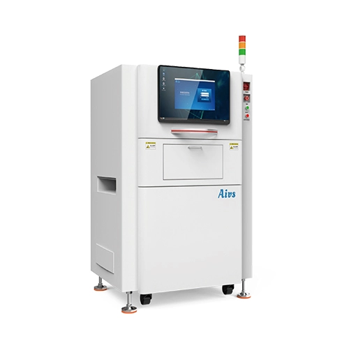
Automated Optical Inspection (AOI) systems play a crucial role in modern printed circuit board (PCB) manufacturing, ensuring quality control and improving production efficiency. Among these, post-wave soldering AOI systems are particularly advantageous for detecting defects in through-hole and surface-mount components after wave soldering. In this blog post, AlVS, as a high performance 2D AOI system supplier, will share the performance advantages of post wave soldering AOI system for sale.
Post Wave Soldering AOI System Performance Advantages
1. High Detection Accuracy and Reliability
Post-wave soldering AOI systems leverage advanced imaging technologies, including high-resolution cameras and multispectral lighting, to accurately identify soldering defects. Key benefits in defect detection include:
– Superior Solder Joint Inspection: Post-wave AOI systems utilize 2D and 3D imaging techniques to assess solder joints with high precision. This includes analyzing parameters such as solder wetting, fillet formation, and joint integrity.
– Enhanced Algorithmic Processing: Machine learning and AI-driven algorithms improve defect classification and false call reduction, ensuring higher accuracy in identifying non-conforming solder joints.
– Comprehensive Defect Coverage: Common defects detected by post-wave AOI include insufficient solder, solder bridging, cold solder joints, and component misalignment, helping manufacturers maintain high-quality standards.
2. Increased Throughput and Efficiency
One of the primary concerns in high-volume PCB manufacturing is maintaining throughput without compromising quality. Post-wave soldering AOI systems address this by:
– High-Speed Image Processing: State-of-the-art AOI systems use parallel processing and high-performance GPUs to analyze images in real time, reducing inspection cycle times.
– Automated Defect Classification: Advanced defect classification algorithms minimize manual review, reducing operator intervention and accelerating defect resolution.
– Seamless Inline Integration: These AOI systems are designed to be integrated directly into the production line, ensuring that PCBs are inspected immediately after wave soldering, preventing defective boards from advancing further in the process.
3. Reduction in Scrap and Rework Costs
Defective PCBs can lead to significant production losses and increased rework costs. A post-wave soldering AOI system helps mitigate these issues through:
– Early Defect Detection: Identifying defects immediately after wave soldering enables manufacturers to take corrective actions before final assembly and testing, reducing costly rework.
– Statistical Process Control (SPC) Integration: AOI systems provide real-time defect trend analysis, allowing manufacturers to fine-tune process parameters and optimize wave soldering conditions.
– Minimized Operator Dependence: By automating the inspection process, AOI systems reduce reliance on human inspectors, eliminating subjectivity and improving repeatability.

4. Adaptability to Various PCB Designs and Configurations
Post-wave soldering AOI systems are designed to handle a wide range of PCB designs, including:
– High-Density Interconnect (HDI) Boards: These systems can inspect densely populated PCBs with complex soldering requirements.
– Mixed Technology Assemblies: They effectively analyze PCBs containing both through-hole and surface-mount components.
– Multiple Soldering Processes: AOI systems can accommodate PCBs soldered using single, dual, or selective wave soldering methods, enhancing their versatility in diverse manufacturing environments.
5. Enhanced User Interface and Software Features
User-friendly software interfaces and advanced visualization tools improve the overall usability of post-wave soldering AOI systems. Key software advantages include:
– Graphical User Interface (GUI) Enhancements: Intuitive touch-screen controls and customizable inspection workflows streamline operator interactions.
– Automated Recipe Creation: Intelligent software tools allow quick and easy setup for new PCB designs, reducing programming time.
– Defect Review and Analysis Tools: Operators can efficiently review inspection results, classify defects, and implement corrective actions using built-in analysis tools.
Conclusion
Post-wave soldering AOI systems offer a multitude of performance advantages, including high defect detection accuracy, increased throughput, reduced scrap and rework costs. These systems play a critical role in ensuring PCB manufacturing quality while optimizing production efficiency. As technology continues to evolve, post-wave soldering AOI solutions will become even more advanced, further driving the automation and reliability of electronics manufacturing processes.
-
AuthorPosts
- You must be logged in to reply to this topic.